
RLS Services – Wafer Probing and Chip-on-Board Packaging Solutions
From wafer sorting to COB assembly, we enable fast, reliable and traceable chip manufacturing in Europe.
RLS Services – Wafer Probing and Chip-on-Board Packaging Solutions
From wafer sorting to COB assembly, we enable fast, reliable and traceable chip manufacturing in Europe.
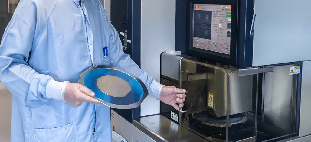
RLS is a leading European technology company with decades of experience and in-house R&D and manufacturing of rotary and linear magnetic encoders. Our new Semiconductor Services division brings this expertise to the world of wafer testing, dicing, die bonding, wire bonding and encapsulation — all in a certified ISO 8 clean room environment in Komenda, Slovenia.
We help fabless semiconductor companies, startups, and specialised industries to shorten time to market and reduce CAPEX by offering flexible, high-quality pilot production and low-volume processing services.
Our capabilities
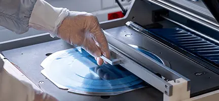
Wafer sort
- Fully automated wafer probing
- Test range from −40 °C to +150 °C
- Heatmaps, Cp/Cpk analysis, .csv data export
- Custom test electronics and fixtures
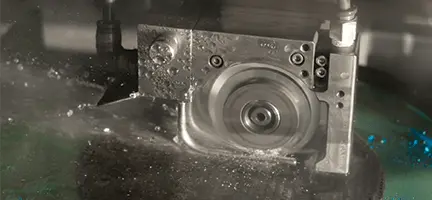
Wafer dicing
- Automatic wafer dicing
- Wafer size up to 8"
- High-precision cutting with ±3 µm accuracy
- 8 inch Disco type frames
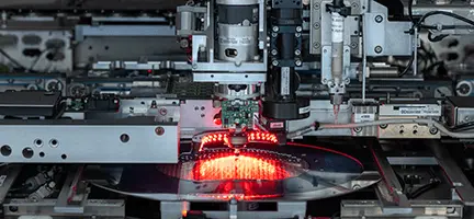
Die attach
- ±10 µm placement accuracy
- Programmable bond force
- Shear test for quality assurance
- Conductive or nonconductive adhesive
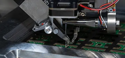
Wire bonding
- Ultrasonic bonding with up to 7 wires/sec
- Al wire
- Pull testing for quality assurance
- Plasma cleaning
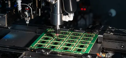
Encapsulation
- Precise material dispensing with closed control loop
- Underfill, globtop, dam & fill
- High temperature encapsulation materials
- Optical clear encapsulation possible
Why choose RLS?
European quality, faster delivery
Avoid long shipping times and customs delays — all packaging is performed locally in our 200 m² ISO 8 clean room, ensuring fast, reliable turnaround across the EU.
End-to-end in-house packaging
From wafer to reel, we handle the entire process — including dicing, bonding, encapsulation, and tape & reel — for consistent quality and full traceability.
Custom engineering and tooling expertise
We support your project from design-for-test to substrate selection, with in-house fixture development and advanced chip-on-board and optical integration capabilities.
Scalable pilot production
Perfect for prototyping, MPW runs, or low-volume production — ideal for medical, industrial, and automotive applications.
Responsive local support
Work directly with our engineering team — no time zone delays or language barriers.
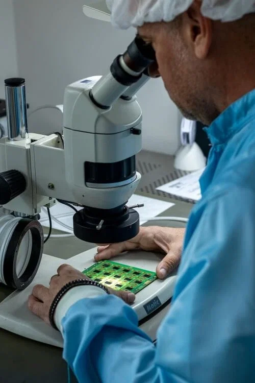
Industries we serve
Medical technology
Automotive industry
Industrial sensors and IoT
MEMS, photonics and custom ASICs
